Semiconductor production needs very clean process conditions. Tiny impurities can affect device quality. Trace organic carbon is one such impurity. It enters water and surfaces during fabrication steps. The industry tracks it closely to protect yield. Now this topic links process control with final output quality. Understanding this link helps improve production consistency.
Nature of Trace Organic Carbon in Fabrication
Trace organic carbon refers to small organic residues in water streams. These residues come from materials and process chemicals. Some residues form during cleaning or rinsing stages. Others arrive from environmental exposure or system components. The presence of carbon compounds can change surface chemistry. This change affects film growth and pattern accuracy. So, engineers monitor these levels in process fluids carefully. Reliable control depends on stable purification systems and proper maintenance.
Interaction with Wafer Surfaces and Films
Organic carbon interacts with wafer surfaces in subtle ways. Thin films require clean and reactive surfaces. Contamination blocks active sites on silicon or metal layers. This blocking reduces uniformity during deposition steps. Sometimes carbon residues form unwanted bonds with surface atoms. Such bonding changes electrical properties of final devices. The effect becomes stronger in advanced nodes with tight tolerances. Now surface defects may not appear visible during inspection. Yet hidden changes still impact device performance later. Careful surface preparation reduces these risks.
Impact on Yield and Defect Formation
Yield measures the percentage of functional devices per wafer. Trace organic carbon lowers yield through defect creation. Organic residues can form particles or stains on surfaces. These defects disrupt lithography and etching accuracy. Misaligned patterns reduce circuit reliability. So small contamination leads to large production losses. The impact grows as device dimensions shrink further. Sometimes contamination also affects dielectric integrity and leakage behavior. This leads to early failure in testing stages. Process engineers must identify sources quickly to avoid yield decline.
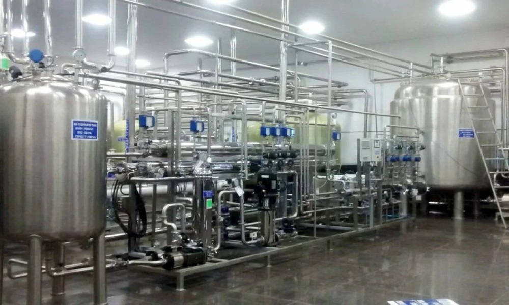
Role of Water Purity and System Design
Water purity plays a central role in contamination control. Fabrication plants rely on high purity water systems for cleaning steps. These systems remove organic carbon and other impurities. Effective filtration and oxidation units reduce contamination levels. But system design must match process requirements closely. Regular monitoring ensures stable performance over time. The selection of materials in piping also affects carbon release. Now maintenance routines help prevent buildup inside the system. Clean water supports consistent wafer processing and reduces defect risk.
Strategies for Monitoring and Reduction
Accurate measurement tools detect trace organic carbon levels in real time. Sensors track changes and alert operators to deviations. Process control systems adjust conditions based on these signals. Sometimes advanced oxidation methods break down organic compounds effectively. Engineers also optimize chemical usage to reduce residue formation. Proper storage and handling of materials limits contamination sources. So coordinated control across systems improves overall yield performance. Continuous improvement efforts refine these strategies further.
Conclusion
Trace organic carbon has a clear impact on semiconductor yield rates. Even small levels influence surface chemistry and defect formation. Clean water and controlled processes reduce these effects significantly. Strong monitoring systems support stable production outcomes. The industry continues to refine methods for better contamination control. This focus helps maintain high yield and reliable device performance.